Introduction
Although the principle of the Metal-Oxide-Semiconductor Field-Effect Transistor (MOSFET) was recognized in the 1920’s, it was not until 1960 that the device was successfully realized. That realization depended critically on the unique properties of the properly processed Si/SiO2 interface, which exhibits a degree of perfection that is difficult to match. That materials system has sustained the microelectronics industry ever since. As devices have shrunk, getting faster and using less power, the SiO2 gate oxide has been successfully reduced to less than 25 Å thick. That scaling process will soon end.
Drivers For Scaling
The “scaling” of device dimensions describes the simultaneous reduction of all of the linear dimensions of the device, and crudely describes the history of the MOSFET from its early day to the tiny devices of today. With gate lengths around 100 nm, today’s MOSFETs can be packed by the millions into a square centimeter of silicon, and at the same time dissipate less power and run faster than their larger predecessors.
There are two primary drivers for reducing the gate oxide thickness during scaling. First, retaining control of the channel to reduce short-channel effects, and second, maintaining high drive current as gate voltage is reduced.
The low power consumption of complementary MOS (CMOS)
circuits reflects the very low current with zero gate voltage applied – orders of magnitude less than when they are
turned on. For the gate to turn the device off, it must be much closer to the
channel electrically than are the source and drain contacts at either end. As
the gate length is reduced, the gate oxide thickness must also be reduced.
Modern device design includes many techniques, such as halo implants, for
reducing short-channel effects. These relax somewhat the requirement for oxide
scaling, but do not eliminate it.
In recent years the
operating voltage of integrated circuits has been decreasing along with the
device dimensions, largely to decrease power consumption by the many millions
of transistors on a chip. A reduced gate voltage means reduced charge induced
in the channel, and thus reduced drive current. The reduction of gate oxide
thickness increases the gate capacitance, and allows a smaller voltage to induce
the same channel charge and drive current.
Gate oxide scaling also
carries a penalty, however: a larger gate charge must be provided to charge the
increased gate capacitance. As a result, “gate-loaded” circuits, in which other
transistors provide the main capacitive load to be charged, do not benefit from
gate oxide scaling. Instead, they are slower (due to mobility degradation
discussed below) and consume more power. “Interconnect-loaded” circuits, in
which the load is primarily the fixed capacitance of metal interconnects, run
faster due to the drive current provided by gate oxide scaling.
scalED Gate oxide
The reduction of gate oxide thickness has been astonishingly
successful, so that oxides with a thickness of roughly 20 Å are in manufacture today. Historical concerns
that such thin oxides would surely exhibit pinholes or other defects somewhere
in a cm2 chip have proven
unfounded. Current manufacturing challenges include the need for this 20-Å-thick oxide to prevent boron–which is present at the 1020 cm-3
level in the p-type gate–from
entering the substrate at even a 1012 cm-2 level during processing at 1000°C or more.
Even measuring this boron penetration is a serious challenge, and electrical
measurement of processed transistors is the most sensitive test. So far,
suitable process design and the introduction of small amounts of nitrogen into
the gate oxide have avoided this problem. However, even more difficult problems
are coming.
Fundamental Limitations
In the idealized scaling scenario, the operating voltage and
dimensions are reduced by the same factor, so that electric fields are
constant. In practice, however, the voltage has been reduced less rapidly than
the dimensions, so the fields have dramatically increased, including the field
across the gate oxide. This has raised important concern about the reliability
of the gate oxide, as it becomes thinner. Indeed, one widely cited paper [[1]]
suggested that oxides would begin to fail for oxides even above 20 Å. The mechanism for this failure is the gradual
buildup of defects associated with carriers accelerated by the gate voltage.
Failure occurs when, somewhere on the chip, enough defects are created in a
small region that they form a highly conductive path, resulting in more
defects, positive feedback, and increased gate leakage. Fortunately, as
clarified by Weir [[2]],
the situation is less dire, because the time to breakdown increases more
rapidly for low voltages than had been expected. Current predictions [[3]]
suggest that, down to about 15 Å, fewer than 100 ppm of chips will suffer
a failure when subjected to operating conditions for ten years, but how much
further this can be assured is unknown.
A second, simpler limit
to oxide scaling is the leakage current through the gate oxide due to quantum-mechanical
tunneling through the oxide. When this leakage current exceeds the off current
of the transistor, the power dissipation of the chip will increase
significantly. For example, for a device with a gate length of 100 nm, an off
current of 1 nA/µm corresponds to a gate current density of about 1 A/cm2.
This has traditionally been regarded as the “limit” of gate oxide leakage, and
corresponds to an oxide thickness of about 14 Å at 1 V [[4]].
It should be noted that
this limit depends strongly on the application. For high-performance
microprocessors, leakage of 100 A/cm2 may be tolerable [[5],
[6]].
Certainly such leakage poses no threat to the operation of most circuits. (Of
course, the reliability of such chips remains an issue.) On the other hand,
applications requiring low standby power, such as cell phones, may require
substantially lower current to maintain acceptable battery life [[7]].
Interestingly, this means that the microprocessor manufacturers may not be the
first to solve the leakage problem.
Diminishing Returns
Even as the scaling of the gate oxide becomes more difficult, it becomes increasingly ineffective at improving performance. We have already noted that only interconnect-loaded circuits derive full advantage from the increased drive current provided by reduced oxide. Two other effects limit even this advantage: electrical corrections to the effective thickness, and mobility degradation at high fields. Interestingly, both of these effects also limit the usefulness of possible replacements for SiO2.
The capacitance per unit area between the gate and the
inversion layer in the substrate is C’=eoxeo/Telec, where eox
is the dielectric constant of SiO2 (3.9), eo
the permittivity of free space, and Telec
the electrical thickness. This thickness is the effective distance between the
centroids of the charge in the gate and the substrate, and includes the
effective thickness of the inversion layer and of the charge sheet in the gate.
A process that achieves high doping of the poly-silicon gate (>1020cm-3)
can limit the latter to 1-2 Å of equivalent
oxide. The effective thickness of the inversion layer will always be 3-6 Å,
however (depending on gate field). This intrinsic capacitance limitation will
always limit the effectiveness of gate oxide scaling [[8]].
(Interestingly, the low in-plane effective mass of electrons in III-V
materials, which allows them superior mobility, also results in a more
stringent limitation on the gate capacitance.) Since the electrical thickness
will always be 4-8 Å thicker than the physical oxide thickness, doubling the
capacitance of a 20-Å physical oxide requires reducing the thickness to 6-8 Å!
As the oxide thickness
is reduced, the increased oxide field pulls the carriers ever more tightly
against the interface. This results in decreased carrier mobility, primarily
due to increased phonon scattering for more confined carriers. (At very high
fields, there is an additional decrease of the mobility due to interface
roughness scattering.) As a result, the current drive will not increase as
rapidly as the capacitance would suggest, and may even decrease with decreasing oxide thickness [[9]],
at fixed supply voltage. This scattering may also degrade transport in the
high-field regime appropriate to sub 50 nm MOSFETs [[10]],
so there may be limited benefit to scaling gate oxides much beyond the current
dimensions.
High-k gate dielectrics
The rapid pace of the silicon industry means that the
difficulties with gate oxide scaling will become critical within a few years at
most. Extensive worldwide effort is focussed on finding a replacement. Because
the goal is continued increase in capacitance, this search is focussed on
materials with a higher dielectric constant (“k”)
than that of SiO2, while retaining its many attractive features.
Since SiO2 has been the key material driving the microelectronics
revolution, its replacement poses significant risk. The challenge is
particularly acute since the electrical thickness must be equivalent to less
than 15 Å of SiO2 to be at all
useful. Given the current feverish pace of research on high-k gate dielectrics, any specific statements are
likely to be irrelevant before they are published. However, some significant
challenges are clear:
Leakage current: The whole point of replacing SiO2 is
to achieve increased capacitance with reduced leakage current. The silicon
conduction and valence band lie near the center of the 9-eV SiO2 band
gap, which means there is a large potential barrier for both holes and
electrons. Since high polarizability at high frequency usually requires an
electronic polarization resulting from a small band gap, alternate materials
will generally show more leakage for the same physical thickness. However, the
overall leakage/capacitance tradeoff can still favor the alternatives.
Reliability: Even after thirty years, the
reliability of SiO2 is a subject of research and vigorous debate.
There is very little data on the reliability of proposed high-k alternatives. It is possible that the mechanisms
limiting reliability will be entirely different.
Interface quality: The electrons and holes in the transistors move
immediately adjacent to the gate dielectric. Any electrical defects (e.g.
interface states) or excessive scattering at the Si/dielectric interface may
compromise the improved performance. On the other hand, introducing a few-Å SiO2
layer at the substrate to mitigate these effects may squander any
capacitance advantage.
Flat-band voltage shift: Almost all of the candidate replacements
exhibit a large (several hundred mV) voltage offset compared to SiO2,
generally attributed to fixed charge in the “bulk” of the dielectric. Attaining
appropriate thresholds in spite of this shift requires changes in the gate
material, device structure, or both. More importantly, the voltage must be the
same for all transistors on a wafer, to a precision of mVs.
Materials compatibility: An alternative gate dielectric stack must exist
in contact with both the substrate silicon and the gate material (currently,
doped polycrystalline silicon). If we consider a metal oxide MOx dielectric,
reactions with the substrate include silicon oxidation Si+MOx ® M+SiO2 and silicide or silicate
formation. Even a very limited reaction could drastically impact the electrical
performance of a 15 Å equivalent film. When such reactions are not allowed [[11]],
the vast majority of possible replacements are eliminated. Moreover, to reduce
the gate contribution to the electrical thickness, metal gates are being considered,
introducing a whole new set of detrimental reactions. Other compatibility
issues concern the need for the dielectric to act as a diffusion barrier to
prevent further substrate oxidation and dopant penetration. Also, the process
to form the dielectric must avoid the formation of adventitious interfacial
layers, even a few Å of which would eliminate the motivation for the
replacement.
Process
compatibility: Current
processes, which introduce the dielectric early in the process, expose the
dielectric to a brief (a few seconds), high-temperature (>1000°C) source/drain activation anneal. The dielectric
must be stable against recrystallization as well as any of the reactions
discussed above. Alternative processes are possible, in which the dielectric is
not formed until after the source/drain activation. One such “replacement-gate”
process is discussed below.
On the whole, there is a huge amount to be learned about the replacement for SiO2 as the gate dielectric, beginning with the most critical: what material will it be? Conventional wisdom states that it takes a decade to generate this knowledge and create the processes and tools needed to implement it. Unfortunately, scaling of conventional SiO2 will be in trouble long before that time has passed.
vertical replacement gate
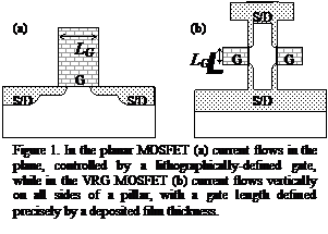
At this point we return to the original drivers for gate oxide scaling:
enabling transistors with shorter gate length, and increasing the drive
current. As we have discussed, attaining these benefits within the conventional
CMOS process, either by reducing the SiO2 thickness or by
replacing it, will become extraordinarily difficult in the next few years. We
have devised an alternative process for transistor formation, the Vertical
Replacement Gate (VRG) process. We will argue that this process provides many
of the same benefits even without oxide scaling; scaling or replacing the gate
dielectric will compound these benefits. While even small changes in
well-established processes are only adopted when the status quo becomes
unacceptable, the challenges of the coming era may constitute a situation where
even more dramatic changes must be considered.
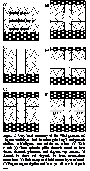
The VRG Process Flow
We present here only a highly simplified version of the VRG process flow, aimed at producing either NMOS or PMOS transistors. A more detailed description can be found elsewhere [[12]].
The primary motivation for the vertical transistor was the definition of the gate length of the transistor by a deposited film thickness (the central, sacrificial layer of the stack illustrated in Fig. 2). This should allow much more precise control of this critical dimension than the ordinary process of lithographic patterning and etch, especially as gate lengths go well below 100 nm. At the same time, by using a replacement-gate process flow, a traditional SiO2 gate oxide can be grown on single-crystal {100} Si; already high-quality 25-Å oxides have been demonstrated [[13]]. In addition, the source and drain extensions are formed by solid-source diffusion from the top and bottom layers of the stack. This self-aligned process allows low series resistance and low gate-source and gate-drain parasitic capacitances. The VRG process is the first to combine these customary attributes of planar MOSFETs with the gate-length control and geometrical advantages of a vertical structure. (We will discuss only the VRG process, but other proposed processes [[14],[15],[16],[17],[18],[19],[20]] may have similar advantages.) To clearly evaluate the leverage provided by geometry alone, in the following we assume that the bare VRG MOSFET will be equivalent to a planar MOSFET of the same gate length. Results to date have fallen a few tens of percent short of that goal for the shortest devices, possibly due to extrinsic effects that should be minimized by optimized processing.
Increased Current Drive
For planar MOSFETs, the current drive is normalized to the
device width. The on current (at VGS=VDS=VDD)
per µm of gate width (at fixed off
current IOFF (at VGS=0 V, VDS=VDD) per µm) is without question the most widely cited device property. ION provides a simple way to
compare transistors from different investigators, to evaluate the effectiveness
of various process choices. Moreover, ION
provides a simple surrogate for the speed performance of interconnect-loaded
circuits, in which the charging of a fixed capacitive load determines the
speed.
Note that for any particular interconnect-loaded circuit, doubling the width of the transistor could also increase the speed, so the value of ION as a speed surrogate may seems illusory. The reason it is in fact meaningful is that there are serious constraints on increasing the transistor width, arising because such an increase would also result in an increase in area. First, the area increase would in turn allow fewer transistors to be packed into the same area of silicon, increasing the cost. Second, if the packing density is limited by the transistors, widening them will increase the length of interconnects and thus their capacitance, further slowing the circuit. Evaluating these issues requires evaluation of dozens of detailed layout design rules. It has been shown [[21]] that selective optimization of gate widths can have dramatic effects on circuit speed and power. Nonetheless, for any given layout methodology, increasing ION per µm of gate width will increase the circuit speed of an interconnect-loaded circuit. As noted above, this has been a major driver behind gate oxide scaling.
It should be clear from this discussion that ION per µm of gate width is useful because it is a surrogate for ION per µm2 of transistor area. The latter normalization more closely approximates the circuit speed implications of the drive current. However, this metric depends on many other design rules that may vary from company to company, and also depends in detail on the particular circuit and the layout style, making the metric ION/µm2 problematic for comparisons.
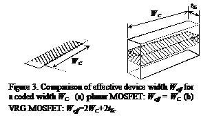
For the VRG MOSFET (as well as other alternative structures), the question of
the appropriate metric for drive capability is critically important, because a
pillar of coded width WC
has a perimeter of at least 2WC. We believe that the
current per unit area is the quantity of real interest, but estimating the area
requires design rules. This in turn requires a complete CMOS process flow. We
have explored a reference VRG CMOS process [[22]]
in which VRG NMOS and VRG PMOS are created side by side. Integrating NMOS and
PMOS requires important changes from a single-polarity process. For example, in
the original NMOS demonstration [12], the channel was doped during growth. For CMOS, as
well as for acceptable VT
control, the channel doping should be performed by implantation. This has now
been successfully accomplished [13]. Other key process steps remain to be exercised, and
experience may dictate changes in the process. The proposed process requires
fewer than four litho levels more than planar CMOS (out of a total of more than
twenty).
Design rules are constrained by manufacturing tolerances and yield as much as by device physics. For the reference flow, almost all of the rules have clear analogs in the planar process, and were assigned the corresponding value for the 0.25-µm design we considered. A handful of rules were set according to educated guesses. All together, some thirty design rules played a role in the overall layout. The gate length plays an important but not a dominant role in the density of planar CMOS. For VRG, the gate length is completely decoupled from the density; the channel thickness tSi (probably comparable to the planar gate length) plays a similar role in layout density.
We compared the layout of a two-input AND gate in a planar 0.25-µm process, and the reference VRG-CMOS process with compatible design rules. Exactly the same coded width of each type of transistor could be placed into the standard cell area. In this sense, neither a large advantage nor disadvantage of the vertical geometry was seen. In terms of perimeter per unit area, therefore, the VRG layout had more than twice the density. Thus, if the drive current of VRG per unit perimeter is the same as for planar, the drive per unit area is roughly doubled, as would the speed with which this AND gate could drive a fixed capacitance.
This rather lengthy argument, relying heavily on realistic layout in a credible
CMOS process, is the foundation of our belief that coded width, not perimeter,
is the best surrogate for device area. This means that the appropriate drive
metric is current per coded gate width.
On this basis, both NMOS [12] and PMOS [13] VRG devices have already surpassed planar devices in
drive current. For interconnect-loaded circuits (where ION matters) the
extra perimeter provided by VRG provides the same advantage as scaling the gate oxide.
It should be obvious from the complexity of the discussion that there are many details of layout, design style, circuit type, and so forth that will alter the real circuit-speed comparison of planar and VRG. Because the precise area is sensitive to many factors, it would not be surprising to see the layout density differ by tens of percent from the precise equality described here. Nonetheless, the use of current per coded gate width provides a useful reference point.
Intrinsic Speed
An important downside to using either oxide thickness or effective width to increase drive currents is the concomitant increase in gate capacitance. When loading by other transistors predominates over interconnect capacitance, the gate capacitance constitutes a majority of the loading, with junction capacitance representing perhaps 1/3 of the total. If the latter were negligible, the circuit speed would be limited by the intrinsic transit frequency of the device, which depends primarily on gate length. In this case, no advantage is afforded by increasing drive current. Indeed, for oxide scaling, because the mobility is degraded at higher fields, gate-loaded circuits becomes slower and dissipate more power as the gate oxide thickness is reduced.
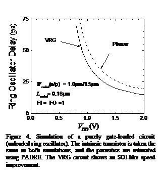
The increased effective width afforded by VRG need not result in mobility degradation, so one might expect to only break even for gate-loaded circuits. (Oxide scaling also raises issues of gate leakage current and reliability that are deferred in VRG.) However, the junction capacitance neglected above can make a big difference to the speed of gate-loaded circuits. Indeed, the difference in junction capacitance is a significant part of the performance benefit promised by silicon-on-insulator (SOI) CMOS. The VRG process was formulated from the beginning to avoid large parasitic capacitances often associated with novel processes. In Figure 4 we show a simulation of the speed of a completely gate-loaded circuit, in which the intrinsic device is exactly the same, but parasitics extracted using the PADRE device simulator are included. The results show that even for gate-loaded circuits, one may achieve SOI-like speed improvements with the VRG process.
Challenges
In spite of the exciting potential described for the VRG process to displace or defer oxide scaling, daunting challenges remain. In the introduction we noted that part of the motivation for gate-oxide scaling is to improve the resistance to short-channel effects. The device engineering to achieve this is currently being explored for VRG, but some of the traditional tools like halo implants are not easily implemented in this process. On the other hand, many of the ill effects of short-channel degradation are problematic only because of the modest gate-length control afforded by current processes. With the much tighter control allowed by the VRG process, one might be able to achieve a performance advantage by tolerating a design that would have been too sensitive to gate length. Moreover, we have already demonstrated [13] scalability of VRG PMOS to 50-nm gate lengths in partially depleted operation with tOX = 25 Å without halos or super-steep retrograde doping. Further improvements are certainly to be expected.
The VRG process makes some of the hardest parts of transistor fabrication easy, but at the same time some of the easy parts get harder. This applies especially to metrology. For example, the traditional ellipsometric measurement of gate oxide thickness becomes impossible, and issues of gate dielectric formation in a narrow confined geometry arise. For example, stress effects or nonconformal deposition can result in serious performance or reliability problems. (These are present in any replacement-gate process). In addition, the two dimensional doping profile resulting from solid-source diffusion should be measured routinely. It may differ substantially from large, planar test structures, and depend on process details such as surface preparation. Many other challenges arise in processing, modeling, and circuit design.
CONCLUSION
The simple reduction of gate oxide thickness to maintain scaling trends in performance is likely to face insurmountable challenges in the next few years. The most likely response of the silicon industry is to introduce a new material for the gate dielectric, but there is still inadequate information to support this approach. The industry may achieve similar ends by introducing a dramatically new transistor structure to achieve higher circuit speeds in other ways.