THE END OF
SCALING: DISRUPTION FROM BELOW
DON MONROE
1. Introduction
The continued scaling of Si CMOS (silicon complementary metal-oxide semiconductor) technology to ever-smaller dimensions faces many critical issues. It is widely believed that these daunting challenges must eventually cause further scaling to slow, and then stop. We discuss an alternative scenario, in which scaling stops, not when it becomes impossible, but when it is increasingly irrelevant to the needs of the mainstream semiconductor market. This scenario has profound implications for warning signs of the end of scaling, and strategies to weather it.
2. Transistor Scaling
According to the National Technology Roadmap for Semiconductors[1],
which embodies the collective wisdom of the
These long-recognized difficulties posed by continued
scaling have engendered numerous predictions of impending saturation of
In this paper, we describe an alternative scenario for the end of scaling, with important implications for the timing and the harbingers of the end of scaling. This scenario suggests very different strategies for negotiating the transition period, as well as the attributes of successor technologies to scaled Si CMOS. In the transition we envisage, the benefits of aggressive scaling of Si become secondary to other attributes, eventually rendering further scaling irrelevant to the mainstream semiconductor market. Naturally, deprived of its historical economic drivers, scaling beyond that point would radically slow as well.
3. Disruptive Technologies
Our description draws on the work of Harvard Business School Professor Clayton Christensen, as summarized in his book The Innovator’s Dilemma[2]. Christensen has analyzed several industries in which leading firms failed to navigate a significant technological shift. In each case, failure resulted not from management failure, or even inability to meet the demands of rapid technological improvement. On the contrary, the firms did an excellent job of understanding the future needs of their most important and profitable customers, sometimes expending enormous effort to make the requisite technological advances. Rather, the firms all experienced failures from below, in which technologies that performed poorly according to the traditional metrics of the industry eventually improved enough to satisfy customers’ needs and win the markets.
|
Figure 1. Disruption in the hard-disk-drive industry. Solid lines represent capacity available for various technologies, while dashed lines represent the capacity actual used by various market segments (adapted from Ref. 2). |

The best-documented example of this disruptive technology is in the hard disk-drive industry[3] as illustrated in Figure 1. Within each market segment, the demand for storage capacity, which the disk-drive manufacturers considered their prime competitive attribute, grew exponentially. Nonetheless, the manufacturers were able to improve capacity even faster. They did not consider physically smaller drives serious competition, because these drives offered much less storage capacity.
The insurgents, with smaller drives, did find eager customers in smaller, emerging technologies that cared less about raw capacity (beyond some minimum) than about other attributes (power, weight, size, etc.) in which the new, small drives excelled. Subsequent capacity improvements (faster than required by either market segment) eventually allowed them to challenge the big drive makers. The former market leaders proved largely unable to meet the challenge from their leaner competitors and were never able to compete successfully in the new markets. Astonishingly, this transition occurred several times in just sixteen years.
|
Figure 2. Incipient disruption in the IC industry? (Drawn from Greg Ledenbach, Intel assignee at Sematech). |
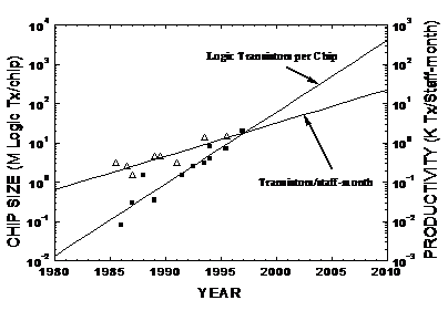
Most observers from the semiconductor industry initially regard the disruptive technology model as irrelevant to our industry, with its insatiable appetite for bandwidth, processor speed, memory, and so on. The idea of technology improving faster than the market demands or can absorb therefore seems foreign. Our environment feels more like that of Lewis Carroll’s Red Queen, running as fast as we can simply to stay in the same place. This perception may be dangerous, however. After all, hard drives compete in very much the same “insatiable” environment! Moreover, as illustrated in Figure 2, there are some indications of performance overshoot in the semiconductor industry as well.
This plot shows rapid improvement (due largely to improvements in Computer-Aided Design Tools) in designers’ ability to produce reliable logic circuits incorporating ever more transistors. Nonetheless, driven by scaling, these improvements are clearly outpaced by the factories’ ability to produce more transistors on a chip. If the designers are the “customers” of the chipmakers, those customers are finding it difficult to absorb further scaling improvements. According to the disruptive technology scenario, scaling is resulting in performance overshoot in a historically critical attribute of ICs: transistor count.
Of course, the precise date of “overshoot” depends on one’s market segment. Comparing the left and right axis, the plot shows a crossover in 1997 for a design effort of 10,000 staff-months/chip. This scale of effort may be tolerable for a microprocessor powerhouse. For other segments that sell chips more cheaply and fewer of each kind, the design costs of maximum-size chips are already excessive.
4.
Microprocessor
Trends
Microprocessors and personal computers have been a primary driver of the microelectronics industry. Since they are also a segment where many of us have daily personal experience, their dramatic evolution has a visceral reality.
Software/Hardware co-evolution
Any PC user cannot help being frustrated by the recurrent obsolescence of computers that had recently seemed entirely adequate. Many regard the huge demand for memory, processor speed, etc. of the latest software as incommensurate with the modest improvements in “productivity” they make possible. For example, the fact that a particular toolbar bounces convincingly and makes an amusing whooshing sound when clicked does not seem like a productivity improvement.
Naturally, power enhancements have enabled such features as the ability to deal gracefully with images and sound on the PC. An objective observer will also recognize the poor quality of many of these representations, and thus the potential for even more processing capacity to improve them, especially if one desires full-motion, high-resolution video on the desktop. Expanded processing power also takes pressure off limited bandwidth resources, allowing real-time compression and decompression of data streams. The computer and software manufacturers have a clear need to convince ordinary consumers of the need for three-dimensional interactive games, real-time image rendering, and other processor intensive applications. Satisfying such voracious increases in demand is the only way to continually sell more powerful processors.
“Segment Zero” Personal Computers.
The recent emergence of low-cost (under US$1000) personal computers is a clear example of disruption, albeit at a higher level than the chip technology. As expected for a disruptive technology, Intel discounted the significance of this market segment early on (although their hungrier competitors did not). Only after the explosive growth of this segment did Intel introduce lower-performance processors specifically targeting this market. These developments do not themselves presage the end of scaling, since even the down-market processors incorporate up-to-date scaled CMOS. What this example does show is that customers (especially in the consumer-electronics market, as in this case) will sometimes forgo steadily improving performance in favor of other attributes, including cost.
5. Implications for Research and Development Strategies
|
Figure 3. Contrast between sustaining and disruptive technology advances. Advances in the current technology (bold solid line) must eventually slow down, allowing a superior but less mature technology (dotted line) to surpass it (given sufficient development resources). Such a transition can sustain the advance of technology as traditionally measured. However, once the current technology exceeds market demands, a disruptive technology (dashed line) providing other advantages may beat out the current technology, even if it is inferior according to traditional metrics. |
Together with anecdotal information, there are some signs of performance overshoot in the less demanding tiers of the IC business. In the rest of this paper we assume that this is a sign that the industry is vulnerable to disruptive transition in the near future, and explore some of the implications of that hypothesis.
“On-The-Roadmap” Research.
The SIA Roadmap publicizes serious challenges facing continued scaling. These challenges include major equipment and infrastructure issues, such as lithography, as well as device and processing questions such as shallow, low-resistance source-drain extensions. The roadmap gives assurance to researchers working on narrower questions that their research will be relevant in the future, and gives them the confidence to explore the difficult, detailed issues that confront proposed solutions. It should be obvious that this confidence is misplaced for technology generations beyond a disruptive transition. In light of the uncertainties of all true research, however, the continued exploration of issues highlighted as potential showstoppers or necessary innovations for the roadmap remain good bets for research. They may not find application as soon as expected in the Roadmap or in the same form, however.
Near-Term Development.
The challenges for nearer-term projects are more serious, since they require substantially greater investments, whose timely recovery is critical to profits. Chipmakers, and to an even greater degree equipment makers, are put at substantial risk by the possibility of a disruptive transition. Interestingly, the very success of the roadmap process will make any such transition especially traumatic, encouraging unwarranted confidence in the momentum of continued scaling as long at is technically possible. Any reduction in the pace of scaling or the market demand will have devastating financial consequences to companies trying to ride the leading edge.
“Off-The-Roadmap” Research.
A large segment of the academic community performs research advertised as technological, but not geared toward extending scaling. Some of this work may enable novel architectures or processing techniques. For example, the architectural principles underlying biological information processing make effective use of parallelism to provide rapid processing with relatively slow devices. Understanding and applying such principles even in relatively antiquated Si technology could improve system performance and power consumption by many orders of magnitude. Research in such areas, while speculative, provides real potential for major breakthroughs
“Beyond-the-Roadmap” Research
. In contrast, significant effort aims to provide “Beyond-The-Roadmap” functionality. The goal is to extend the performance, defined according to the traditional metrics, beyond an expected saturation of CMOS capability, as illustrated by “surpassing technology” in Figure 3. The classic example is III-V electronics, but equally relevant might be single-electron memories, thought to extend memories into the Terabit/cm2 regime. It is axiomatic in the disruptive technology paradigm that such technologies are addressing the wrong question. Well before CMOS has encountered physical limits to scaling, it will have overshot the necessary performance as traditionally measured, and the new differentiating attributes will become important. This is perhaps the most profound conclusion of the scenario described in this paper: “Beyond-the-Roadmap” research is unlikely to be directly useful.
6. Economic Drivers
The performance improvements engendered by aggressive CMOS scaling are well known. They include both direct effects on the transistors–improved current drive and reduced capacitance of scaled transistors–and indirect effects of reduced area–reduced interconnect delays and power for smaller chips. The performance advantages of scaling Si have enabled awesome improvements in CMOS performance, while keeping power consumption modest. However, performance improvements alone would not have justified the massive R&D investments in scaling. The fundamental driver has been reduced cost.
Interestingly, the cost of processed Si per unit area has not changed much: it has remained around $5/cm2 for several decades. The cost that has been following Moore’s law of exponential decrease is the cost per transistor. More commonly, this is expressed as “Cost per Function,” that is, the total chip cost divided by the number of logic gates, or some similar function. Chip cost, however, has not decreased by many orders of magnitude. Rather, customers have been convinced to buy ever more function for roughly the same cost. For example, Marty Lepselter observed[4] that the current generation of DRAM always costs about $p.
Once entire systems on a chip are available, this economics will change. Does it make sense to buy ten systems on a chip? At this point, the relevant quantity will not be “Cost per Function,” but “Cost for MY Function.” If customers stop desiring ever-greater function, continued scaling makes economic sense only if it reduces the cost for a fixed chip size. Disk drives offers a sobering example of this phenomenon: for every one of the new generations shown in Figure 1, the cost per MB (cost per function) was higher for the new drives, when they were introduced. This did not prevent their eventual dominance.
An essential aspect of the economics of scaling is integrating functionality on a single chip. As with device scaling, this includes both performance advantages and economic advantages. These advantages are more complicated, however, when it comes to integrating multiple, disparate device types on a single chip.
Single-chip integration allows increased speed and lower power, as well as more and wider data paths between sections. The speed and power improvements reflect the large parasitics (capacitive and inductive) inherent in traditional packaging technologies. In addition, off-chip connections are subject to uncontrolled terminations and so must accommodate electrostatic discharge, variations in load, etc. The required protection and design margin further increase the area. The large metal pads used for contacts may consume precious Si area. Solder connections and metalization on the board remain much larger than those on the chip, and the packaging overhead can be a substantial contributor to board size. Most of these issues, however, are really shortcomings in inter-chip interconnection schemes, rather than intrinsic drivers for single-chip integration.
Indeed, there are many pitfalls in single-chip integration. The well-known difficulty of providing “known-good die” for multi-chip modules is not solved by integration. Indeed, reduced pin count per transistor only magnifies the testing challenges for large circuits. Even more challenging is the incompatibility of process flow for various types of device, for example, CMOS, bipolar, dense and/or programmable memory, and the capacitors, inductors, and resistors useful in analog applications. In some cases, for example BiCMOS circuits or the integration of NMOS and PMOS to form CMOS, the devices are so interspersed that developing a compatible process flow is compelling. In other cases, the integration is driven by imperfections of interconnection. Traditional CMOS wafers are also a highly flawed environment for isolating sensitive analog circuits from noisy digital circuits. Thus, for some applications, the economic stimulus for integration may weaken before the entire system is on a single chip, if advanced packaging schemes can minimize these inadequacies of the interconnections.
7. Potential Challengers for Scaled CMOS
We believe that in the next few years the overall integration level on a chip will cease to be the most important attribute for IC technology. Identifying the vulnerability of Si scaling to disruption is only the beginning, however. The much harder task is identifying candidates for disruptive technologies that will invade the less challenging traditional and emerging markets. The successful candidate will not be superior in sheer density of transistors or raw transistor speed, but will offer other attributes, including cost for desired function. Following are a few possibilities. Inevitably, without the luxury of hindsight, this list is arbitrary and almost certainly misses important candidates.
Design Productivity and Re-use
Intellectual Property (IP) Movement.
One response to the design productivity gap illustrated in Figure 2 is to try to re-use ever-larger blocks of existing designs in new circuits. While this is a traditional goal within companies, there is a growing trend toward sharing designs between companies (for an appropriate fee). The growing importance of foundries reinforces this trend, as some of them would like to offer not just a process but proven subcircuits as well. It seems clear that designs that function acceptably on a variety of fab lines cannot fully exploit the capabilities of the process. Rather, the goal of optimum performance is traded off for greater flexibility and economy of design resources.
Software implementation on microprocessor.
A well-established route to improve productivity is to re-use the entire microprocessor, and to take advantage of its general-purpose programmability to implement arbitrary functionality in software. This strategy will always be a very effective means to rapid implementation of new algorithms, and provides other advantages such as remote upgradability. To date, however, this strategy has supported, not undercut, increasing microprocessor power, as functionality formerly executed by dedicated chips are performed by the underused microprocessor.
Integration of Diverse Functionality
Modular Processes.
The traditional approach to incorporation of alternate functionality is the inclusion of multiple process modules. At Lucent, this approach is called the “Superchip,” in which each process enhancement, for example, Flash Memory, or BiCMOS, or linear components, is totally compatible with the core CMOS process. So far, these enhancements have been achieved without any sacrifice in performance of the fully scaled, core digital CMOS process. However, developing such compatible processes may become harder.
As a possible leading indicator, one company recently introduced a process optimized for the fabrication of CMOS cameras. This process is far from cutting edge in its CMOS performance, but for those interested in camera functionality that may be of little importance.
MEMS.
Another candidate is the functionality provided by “Micro-electrical-mechanical systems,” or MEMS. While the return to devices with moving parts seems to conflict with the historical strengths of Si ICs, the reliability of such mass-produced parts as accelerometers for airbags suggests otherwise. Moreover, the fabrication techniques include lithographic patterning and wafer-scale processing, leveraging many of the same economies present for CMOS fabrication. In addition, MEMS can potentially provide small, cheap, electronic interfaces to the non-electronic world, including chemical, mechanical, optical, and magnetic signals. Of course, MEMS processing is not easily integrable with CMOS processing. Existing examples of integrated CMOS/MEMS processes do not approach the state of the art, but even relatively archaic CMOS can substantially enhance the usefulness of MEMS.
Multi-chip modules.
As discussed above, there are serious economic and
performance drivers for single-chip integration, but there are also serious
economic and performance drivers against it. Because many performance problems
arise from excessive packaging parasitics, there is continuing interest in
packaging that reduces these parasitics. Imagine a pre-testable chip-scale
package using a low-parasitic, high-density array to contact a compatible board
carrying other chips, including area-hungry passive components. The challenges
of integrating potentially incompatible
processes may not seem as worthwhile.
Optically-coupled ICs.
One strategy for improved packaging is optical
interconnect, with its potentially high speed and low parasitics. As before,
integrating this functionality may not be compatible with the ultimate CMOS
performance and density, but for many applications it may be more important.
Alternative Materials Systems
Organic Transistors.
Si can be expected to remain the king of standard semiconductor applications. A novel materials system must include attributes not necessarily quantitatively better but qualitatively distinct from those of Si CMOS. Organic semiconductors exhibit such attributes. According to traditional metrics, these semiconductors are dreadful, exhibiting mobilities orders of magnitude below those of single-crystal Si, and limited prospects for processing at elevated temperatures. However, they could potentially be printed cheaply on surfaces, including plastics and other flexible materials, and thus used in ways previously unforeseen. The “bendable television” may not seem necessary, but it illustrates the dramatic new possibilities that may become indispensable.
III-V electronics.
It may seem surprising to see III-V electronics, e.g. GaAs, in a list of potential disrupters for Si technology, since disrupters are generally lower performers than the reigning technology. Note, however, that in Figure 3, the challenger lags behind the current leader in the attributes currently valued by the marketplace, so GaAs must currently be inferior. This implies that the actual attribute most valued by the mainstream market is not speed, but overall integration level (and thus cost) as well as power. Imagine a future in which GaAs (currently a niche player for “low-level” applications not requiring the ultimate in power or integration) continues to improve in integration level. As Si overshoots the integration needs of the marketplace, the door is open for other attributes, including raw speed. Naturally, this performance must not violate other market constraints, including cost, and the future for III-V’s in mainstream electronics does not appear terribly bright. We introduce the idea only to emphasize the critical nature of identifying the correct attributes for quantifying “performance.”
Wide bandgap semiconductors.
Semiconductors such as SiC, diamond, and various nitrides have band gaps much larger than Si, and therefore operate well at much higher temperatures. These materials could provide operation in environments unsuitable for Si based electronics.
8. Summary
We have presented here a hint of a future of the semiconductor industry that contrasts sharply with the standard view. In that view, scaling of transistors and interconnect, as envisioned in the SIA roadmap, continues unabated, provided vast increases in the number of transistors on a chip and similarly huge reductions in cost and power per transistor. At the same time, many companies see the highest value added shifting to systems-on-a-chip: the incorporation of processes in addition to digital logic CMOS, notably high-density and/or programmable memory and full-function analog and RF. The standard view assumes that both scaling and systems-on-a-chip will coexist.
We have suggested that the economic incentive for continued scaling will dissipate as the available level of integration of digital components overshoots the demands of a progressively larger fraction of the market. Si will remain the primary materials system for the highly integrated digital functions. The value added will increasingly shift to other functionality.
In the 1984 International Electron Devices Meeting, Marty Lepselter4 likened Si to steel, a material that remains a primary structural material in spite of niche competition from more exotic materials. It is interesting to note that the steel industry was one of those shown by Christensen to have experienced a disruptive transition in recent decades. That transition did not reflect a dramatic improvement in quality; indeed, the new material was generally inferior. Rather, novel factories (“minimills”), widely adopted in the Far East, progressively invaded the lower, less profitable segments of the steel market. Traditional mills, for example in the U.S., eventually lost most of their market. Perhaps a similar fate awaits the leaders of the IC industry today.